Scanning Tunneling Microscope Presentation
| Introduction to Scanning Tunneling Microscope (STM) | ||
|---|---|---|
| The Scanning Tunneling Microscope (STM) is a powerful tool used to observe and manipulate individual atoms on surfaces. It was invented in 1981 by Gerd Binnig and Heinrich Rohrer at IBM Zurich. STM operates based on the principle of quantum tunneling, where an electric current flows between a sharp tip and the sample surface. | ||
| 1 | ||
| Working Principle of STM | ||
|---|---|---|
| STM works by scanning a sharp tip across the surface of a sample while maintaining a small distance. As the tip approaches the surface, electrons can tunnel through the vacuum barrier between the tip and the sample. The tunneling current is highly sensitive to the distance between the tip and surface, allowing for atomic-resolution imaging. | ||
| 2 | ||
| Atomic Resolution Imaging | ||
|---|---|---|
| STM can provide real-time images of the surface with atomic resolution. By scanning the tip in a raster pattern, information about the height and arrangement of atoms is obtained. The STM image represents the topography of the surface, revealing details at the atomic scale. | ||
| 3 | ||
| Manipulation and Nanofabrication | ||
|---|---|---|
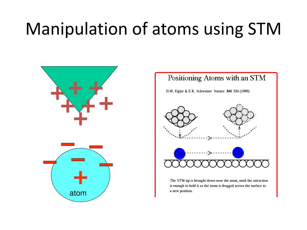
| STM allows for precise manipulation of individual atoms by applying voltage pulses to the tip. By carefully controlling the tunneling current, atoms can be moved, rearranged, or even removed. This capability has opened up opportunities for nanofabrication and the creation of nanostructures with specific properties. | ||
| 4 | ||
| Advantages of STM | ||
|---|---|---|
| STM provides unparalleled resolution at the atomic scale, allowing for detailed studies of surfaces and nanostructures. It can operate under various conditions, including ambient pressure and in different environments. STM can be used on conductive and non-conductive samples, making it versatile for a wide range of material systems. | ||
| 5 | ||
| Limitations of STM | ||
|---|---|---|
| STM requires a conductive sample or the presence of a conductive coating for imaging. The tip-sample interaction can cause damage to the surface, limiting imaging of delicate samples. STM is limited to studying surfaces and cannot provide information about the bulk properties of materials. | ||
| 6 | ||
| Applications of STM | ||
|---|---|---|
| STM has been instrumental in the study of surface chemistry, catalysis, and nanoscale physics. It has played a crucial role in the development of nanotechnology and the understanding of quantum phenomena. STM is used in various fields, including materials science, surface science, and nanoscience. | ||
| 7 | ||
| Future Developments | ||
|---|---|---|
| Advances in STM technology aim to improve resolution and extend capabilities beyond imaging. Combined techniques, such as STM with spectroscopy, can provide valuable information about electronic properties. Integration with other imaging techniques, like atomic force microscopy (AFM), offers complementary imaging modes. | ||
| 8 | ||
| Importance of STM in Scientific Research | ||
|---|---|---|
| STM has revolutionized our understanding of the nanoworld and the behavior of atoms and molecules on surfaces. It has enabled breakthrough discoveries and continues to drive innovation in various scientific disciplines. STM remains a vital tool for exploring new materials, characterizing surfaces, and pushing the boundaries of scientific knowledge. | ||
| 9 | ||
| References (download PPTX file for details) | ||
|---|---|---|
| Binnig, G., & Rohrer, H. (1982). Scanning tun... Eigler, D. M., & Schweizer, E. K. (1990). Pos... Mannhart, J. (2020). Scanning tunneling micro... |  | |
| 10 | ||
| References (download PPTX file for details) | ||
|---|---|---|
| Your first bullet... Your second bullet... Your third bullet... |  | |
| 11 | ||


