Miticating Defects In Ic Fabrication Presentation
| Introduction to Mitigating Defects in IC Fabrication | ||
|---|---|---|
| Defects in IC fabrication can lead to performance degradation and device failure. Mitigating defects is crucial for improving yield and ensuring reliable operation of integrated circuits. This presentation will discuss various techniques and strategies for mitigating defects in IC fabrication. | ||
| 1 | ||

| Process Optimization | ||
|---|---|---|
| Optimizing fabrication processes helps reduce defects and improve yield. Understanding the impact of different process parameters on defect formation is essential. Techniques such as Statistical Process Control (SPC) and Design of Experiments (DOE) can be used to optimize processes. | ||
| 2 | ||

| Cleanroom Environment | ||
|---|---|---|
| Maintaining a cleanroom environment is critical for defect mitigation. Controlling particulate contamination and airborne molecular contaminants is essential. Regular cleaning, air filtration, and strict protocols for personnel and equipment minimize defects. | ||
| 3 | ||

| Mask Design and Lithography | ||
|---|---|---|
| Defects in mask design or lithography can propagate throughout the fabrication process. Careful mask layout, design rule checks, and lithography optimization are necessary. Advanced techniques like optical proximity correction (OPC) and phase-shift masks improve pattern fidelity and reduce defects. | ||
| 4 | ||

| Wafer Inspection and Metrology | ||
|---|---|---|
| Regular inspection and metrology help identify defects at various stages of fabrication. Techniques such as optical inspection, scanning electron microscopy (SEM), and atomic force microscopy (AFM) are used. Automated defect classification and defect mapping enable targeted defect mitigation strategies. | ||
| 5 | ||

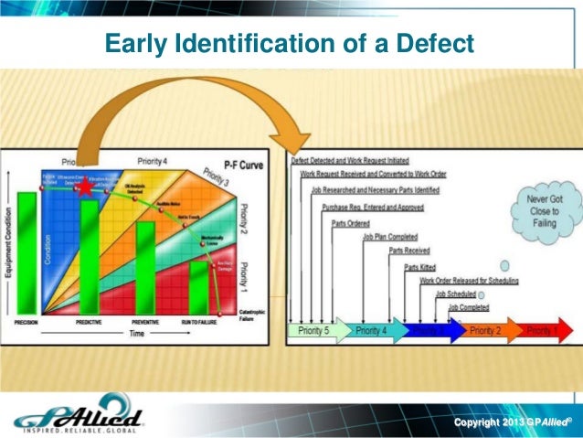
| Defect Detection and Repair | ||
|---|---|---|
| Early detection of defects allows for timely repair or mitigation. Techniques like electron beam-induced current (EBIC) and focused ion beam (FIB) enable defect localization and repair. Advanced defect detection methods, such as laser scanning microscopy, provide higher resolution and detection sensitivity. | ||
| 6 | ||
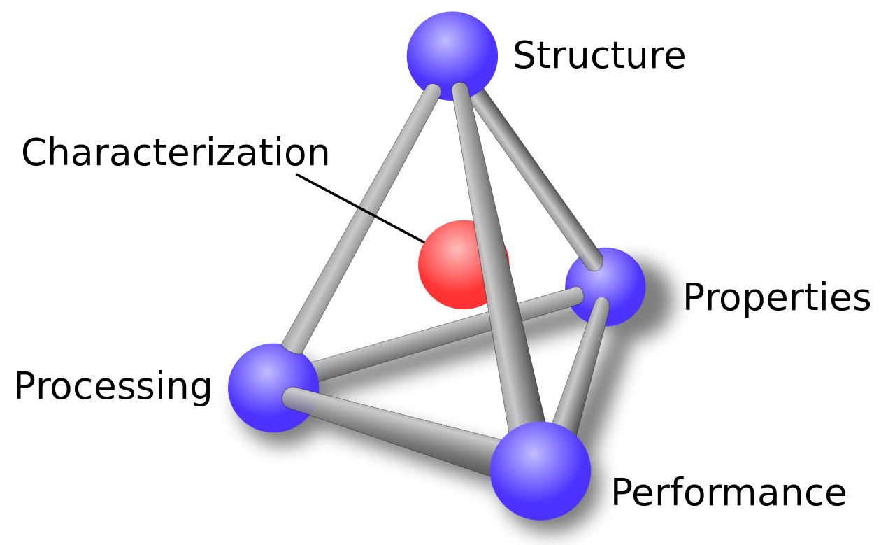
| Material Characterization and Selection | ||
|---|---|---|
| Understanding material properties and their impact on defect formation is crucial. Characterization techniques like X-ray diffraction (XRD) and transmission electron microscopy (TEM) help analyze materials. Selecting materials with lower defect densities and improved stability reduces fabrication defects. | ||
| 7 | ||
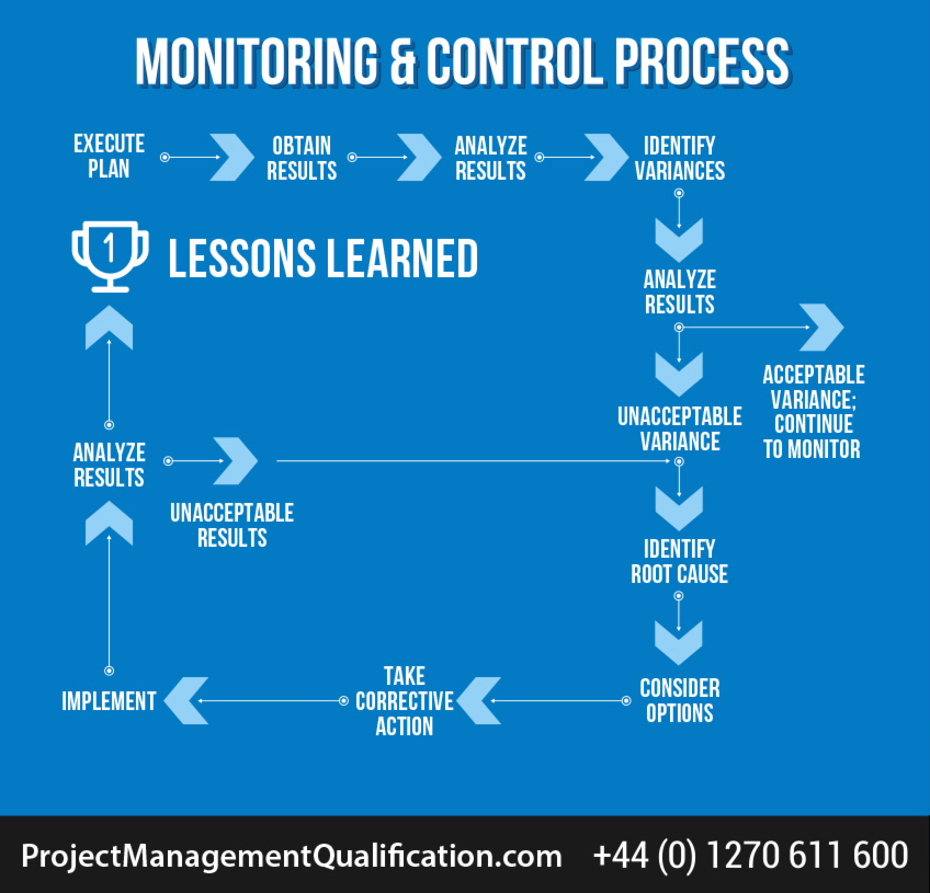
| Process Monitoring and Control | ||
|---|---|---|
| Continuous monitoring and control of fabrication processes are crucial for defect mitigation. Real-time process monitoring techniques, such as in-line metrology, enable proactive defect detection. Closed-loop feedback systems can automatically adjust process parameters to minimize defects. | ||
| 8 | ||
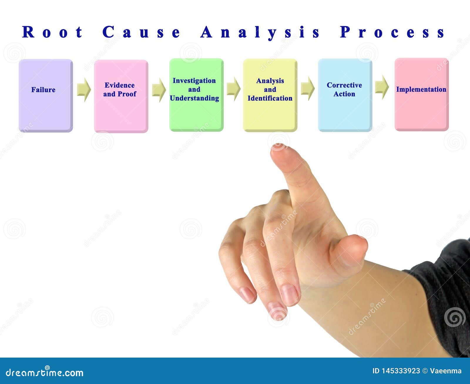
| Defect Analysis and Root Cause Identification | ||
|---|---|---|
| Analyzing defects and identifying their root causes is essential for effective mitigation. Techniques like fault isolation, electrical probing, and failure analysis help determine defect origins. Collaborating with equipment manufacturers and materials suppliers can aid in root cause identification. | ||
| 9 | ||
| Summary | ||
|---|---|---|
| Mitigating defects in IC fabrication is vital for improving yield and device reliability. Process optimization, cleanroom environment control, and mask design/ lithography play key roles. Wafer inspection, defect detection/ repair, material characterization, and process monitoring are critical. | ||
| 10 | ||

| References (download PPTX file for details) | ||
|---|---|---|
| [Insert reference 1]... [Insert reference 2]... [Insert reference 3]... |  | |
| 11 | ||