CMOS Inverter Using VLSI Presentation
| Introduction to CMOS Inverter using VLSI | ||
|---|---|---|
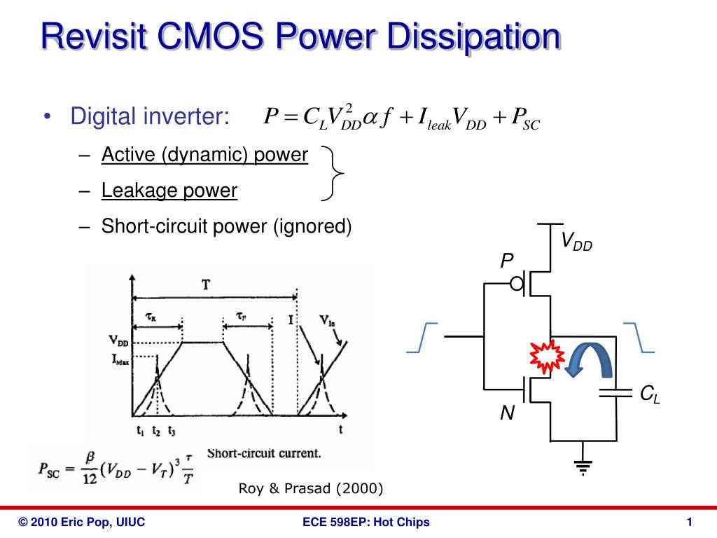
| The CMOS inverter is a fundamental building block in VLSI (Very Large Scale Integration) circuits. It consists of a PMOS (P-type Metal-Oxide-Semiconductor) transistor and an NMOS (N-type Metal-Oxide-Semiconductor) transistor connected in series. The inverter performs logic inversion, converting a high input voltage to a low output voltage, and vice versa. | ||
| 1 | ||

| CMOS Inverter Operation | ||
|---|---|---|
| In a CMOS inverter, when the input voltage is high, the PMOS transistor turns off, and the NMOS transistor turns on, allowing current to flow from the supply voltage to ground, resulting in a low output voltage. Conversely, when the input voltage is low, the PMOS transistor turns on, and the NMOS transistor turns off, blocking current flow, and resulting in a high output voltage. The switching between high and low output voltages makes the CMOS inverter ideal for digital logic circuits. |  | |
| 2 | ||
| Advantages of CMOS Inverter using VLSI | ||
|---|---|---|
| Low power consumption: CMOS technology allows for low power dissipation due to the absence of static current flow in steady state conditions. High noise immunity: The CMOS inverter has a high noise margin, making it less susceptible to noise and disturbances in the input signal. High packing density: VLSI technology enables the integration of a large number of CMOS inverters in a small area, leading to higher circuit complexity and functionality. | ||
| 3 | ||
| CMOS Inverter Layout | ||
|---|---|---|
| The layout of a CMOS inverter involves placing the PMOS and NMOS transistors side by side, with their sources connected to the supply voltage, and their drains connected to the output node. The input signal is applied to the gates of both transistors, controlling their conduction. The output node is connected to the load, which can be further connected to other CMOS inverters or digital logic circuits. | ||
| 4 | ||

| VLSI Fabrication Process | ||
|---|---|---|
| VLSI fabrication involves several steps, including wafer preparation, oxidation, photolithography, etching, deposition, and metallization. The CMOS inverter is built on a silicon wafer, where layers of oxide, polysilicon, and metal are sequentially deposited and patterned to create transistors and interconnects. The use of advanced lithography techniques allows for the miniaturization of transistors, leading to higher integration density. | ||
| 5 | ||

| CMOS Inverter Performance Parameters | ||
|---|---|---|
| Switching speed: The time required for the output voltage to transition from high to low or vice versa. It depends on factors such as transistor sizes, load capacitance, and supply voltage. Power consumption: The energy consumed by the CMOS inverter during operation. It is a function of the supply voltage, transistor sizes, and switching activity. Noise immunity: The ability of the CMOS inverter to tolerate noise and disturbances in the input signal without affecting the output. | | |
| 6 | ||
| Scaling in CMOS Inverter | ||
|---|---|---|
| Scaling refers to the reduction in transistor dimensions to improve performance and packing density. As transistors are scaled down, their size, power consumption, and switching speed decrease, while integration density and speed increase. Scaling also poses challenges such as increased leakage currents and reduced noise margins due to process variations. | ||
| 7 | ||
| Applications of CMOS Inverter | ||
|---|---|---|
| CMOS inverters are widely used in digital logic circuits, such as flip-flops, registers, multiplexers, adders, and arithmetic logic units (ALUs). They are essential components in microprocessors, microcontrollers, memory chips, and other digital systems. CMOS inverters also find applications in analog circuits, such as operational amplifiers and analog-to-digital converters. | ||
| 8 | ||

| Future Trends in CMOS Inverters | ||
|---|---|---|
| Continued scaling: Transistor dimensions will continue to shrink, enabling more complex and powerful VLSI circuits. Low-power design techniques: With increasing emphasis on energy efficiency, researchers are developing new design approaches to reduce power consumption in CMOS inverters. Alternative technologies: Beyond CMOS, emerging technologies such as spintronics, quantum computing, and memristors may offer new possibilities for inverter design. | ||
| 9 | ||
| Conclusion | ||
|---|---|---|
| The CMOS inverter using VLSI is a fundamental component in digital and analog circuits. Its advantages include low power consumption, high noise immunity, and high packing density. With ongoing advancements in VLSI technology, CMOS inverters will continue to play a crucial role in the development of advanced electronic systems. | ||
| 10 | ||
